
What is an example of micro imprinting?
One of the best examples of wafer level optics is the camera module on your mobile phone.
The basic idea is to fabricate layers of microlenses that are stacked up to make the complete optical element, which is then bonded directly onto the image sensor of the camera, at the wafer level.

At left is an image from EV Group, showing an exploded view of the elements of a typical wafer level camera module. (Image courtesy of EV Group –evgroup.com)
These include the polymer lenses, spacers and aperture layers and the CMOS image sensor at the bottom.
Just seeing the photo might make you realize how accurately this device must be made and assembled to work properly. Current imprint technologies enable feature sizes as small as microns and positioning technologies allow position accuracies of sub-100 nm. This is indispensable to the proper alignment of the multiple layers in such tiny modules.
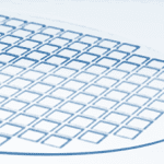
Hundreds are imprinted at a time on a glass wafer substrate (like the one shown at right). Each square on the wafer is a polymeric lens layer. Each layer in the lens stack has its own stamp. The most established wafer-level optics fabrication techniques allow double-sided molding of microlenses onto the glass wafer. The optical imprint resin is dispensed in a layer on the glass wafer. The stamp is aligned, then lowered down onto the resin layer. Controlled squeezing of the resin layer enables continuous filling of all lens cavities across the entire area of the stamp. The resin is cured by exposure to UV light and the stamp is lifted away.
Highly accurate assembly and bond alignment of the multiple layers results in a very compact, highly accurate module that can be mounted directly onto a printed circuit board.In the last 10 years this kind of moldule has essentially replaced the conventional barrel-type cameras.